
Analysis of Combinational Circuit Notes Tutorial with Examples
Combinational Circuit
Combinational circuits are Logic circuits that perform arithmetic functions (e.g., addition, subtraction, multiplication and division).
These circuits don’t have memory and the output depends only on inputs provided. Combinational circuit is a logic circuit containing only logic gates.
Key Points
- Logic gates are not always required because simple logic functions can be performed with switches or diodes.
(a) Switches in series (AND function) (b) Switches in parallel (OR function)
(c) Combining IC outputs with diodes (OR function)
Basic Logic Gates
NOT Gate
- One input, one output
- Whatever logical state (1, 0) is applied to the input the opposite state (0,1 respectively) will appear at output.
- Also known as inverter.

OR Gate
The output will be high / true / 1, if any or all of its inputs are high / true / 1. The output will be low / zero / false only if all of inputs are low / zero / false.

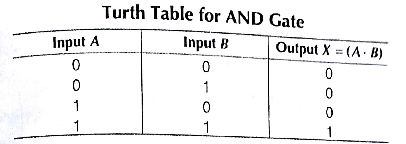
AND Gate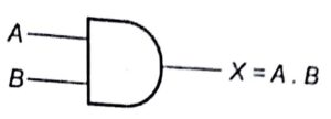
output will be high / true / 1, if all of its inputs are high / true / 1. If any of its inputs is low/false/ 0, then output will be low / false / 0.
To change the type of gate, such as changing OR to AND, you must do three things ,
- Invert (NOT) each input.
- Change the gate type (OR to AND or AND to OR) .
- Invert (NOT) the output.
Universal Gates
Any function can be implemented with the help of these (NAND, NOR) gates.
NAND Gate
This is an AND gate with the output inverted or we can say (AND + NOT). Therefore, the output expression of the two input NAND gate is X = (A . B)’.

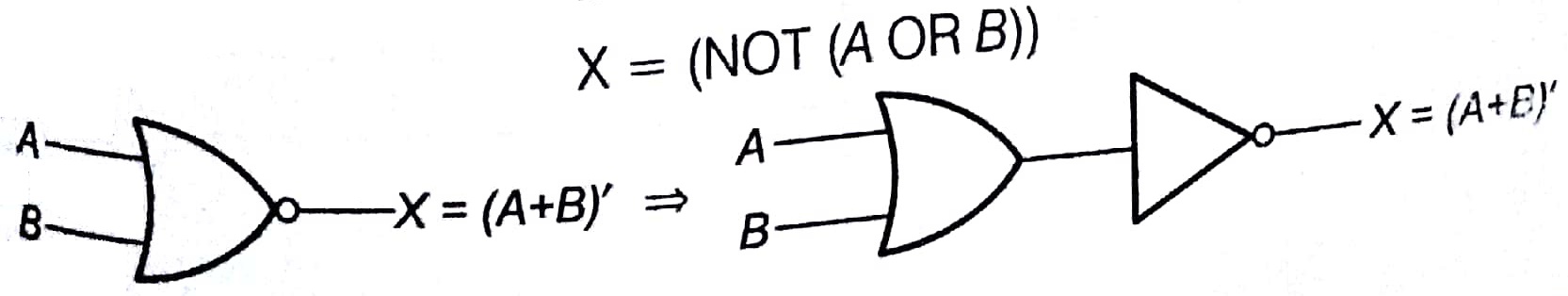
NOR Gate
This is an OR gate with the output inverted or we can say (OR + NOT). °re, the output expression of the two input NOR gate is X = (A + B) . we ref X (NOT (A OR B))

Other Types of Gates
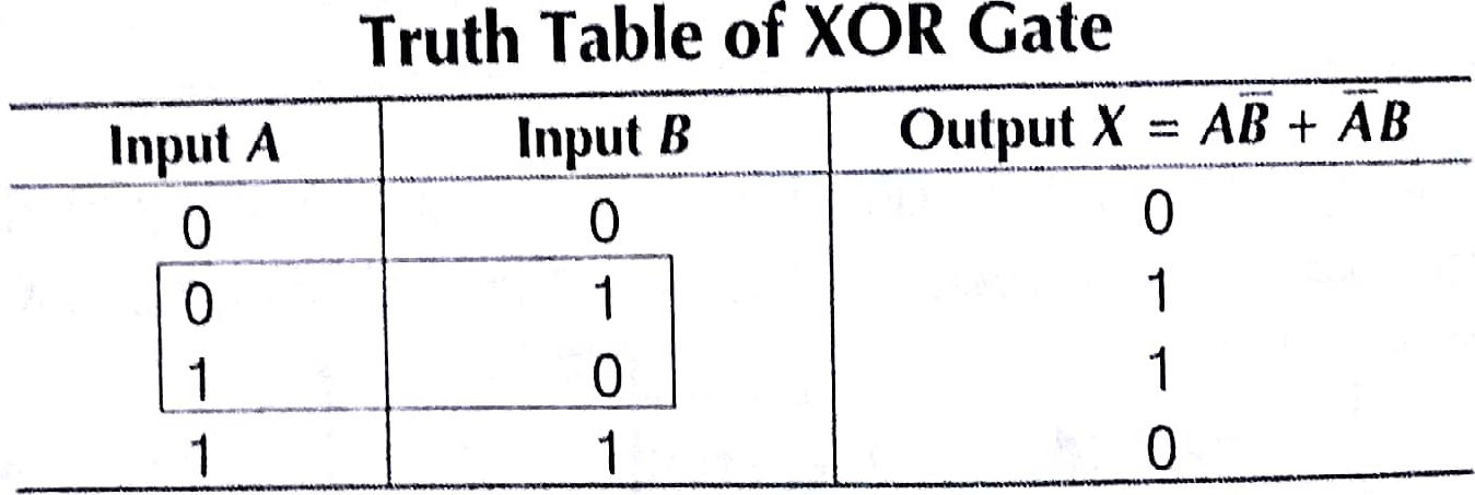
Exclusive OR (EX-OR / XOR) Gate
The XOR gate provides 1 as an output only if its two inputs are different. If the inputs are same, the output will be a ‘0’. Unlike 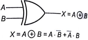 standard OR / NOR and AND / NAND functions the XOR function always has exactly two inputs.
X=A+B=A•B+A•B
If A and B are different, then the output will be high.
Exclusive NOR (EX- NOR / XNOR) Gate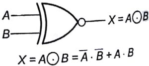
The XNOR gate produces output 1 only if the inputs are same. If the inputs are different the output will be a zero 0.
X=A•B=A•A+A•B
If A and B are different, then the output will be low or zero.

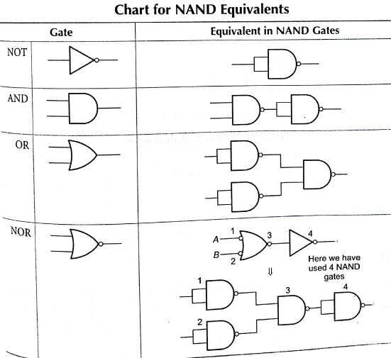
Substituting one Type of Gate for Another
Any Logic Gate can be built from NAND or
NOR Gates
NAND or NOR gates can be combined to create any type of gate. This enables a circuit to be built from just one type of gate, either NAND or NOR. e.g, an AND gate is a NAND gate, then a NOT gate (to undo the inverting function).
Key Points
- AND and OR gate can’t be used to create other gates because they lack the inverting (NOT) function.
e.g., an OR gate can be built from NOTed inputs fed into a NAND ( AND + NOT) gate.
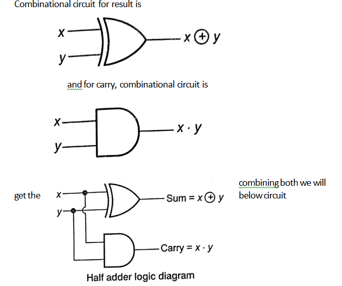
Combinational Circuit for Arithmetic Operations
Half Adder
Addition of 2 binary digits requires 2 inputs and 2 outputs, one for result and one for carry.

Full Adder
A full adder is a combinational circuit that forms the arithmetic sum of 3 input bits. It consists of 3 inputs and 2 outputs. Two of the input variables are the 2 significant bits to be added. The 3 rd input represents the carry from previous lower significant position.
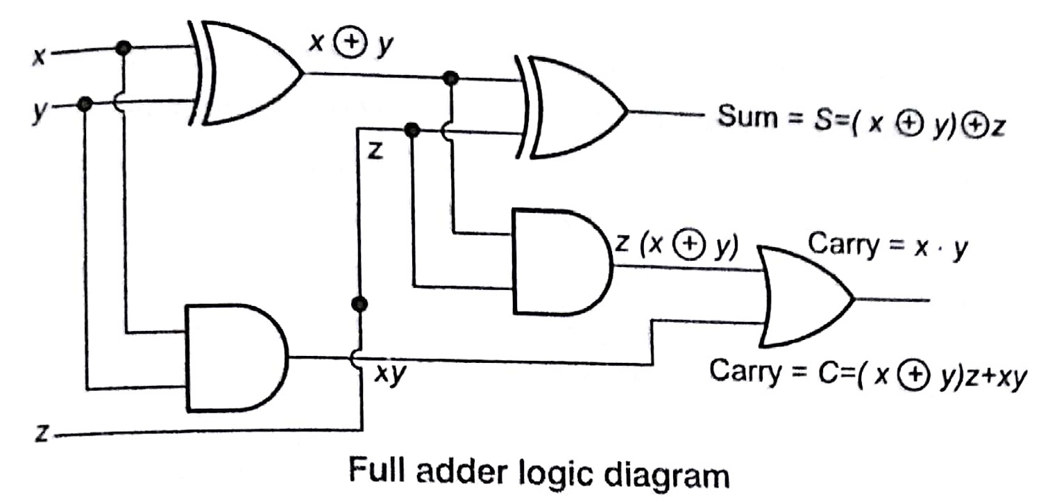
S = Z ED (X @ y) = z’ (xy’ + x’ y) + z (xy’ + x’ y)’
S = z’ (xy’ + x’ y) + z (xy + x’ y’ )
S = xy’ z’ + x’ yz’ + xyz + x’ y’ z
and the carry output is C = z (xy’ + x’ y) + xy = xy’ z + x’ yz + xy
Positive and Negative Logic
- If the signal that activates the circuit (the 1 state) has a voltage level that is more positive that the 0 state, then the logic polarity is considered to be positive. Thus, in positive logic 1 is considered as high value and 0 is considered as low value.
- If the signal that activates the circuit (the 1 state) has a voltage level that is more negative than the 0 state, then the logic polarity is considered to be negative. Thus in negative logic 1 is considered as low value and 0 is considered as high value.
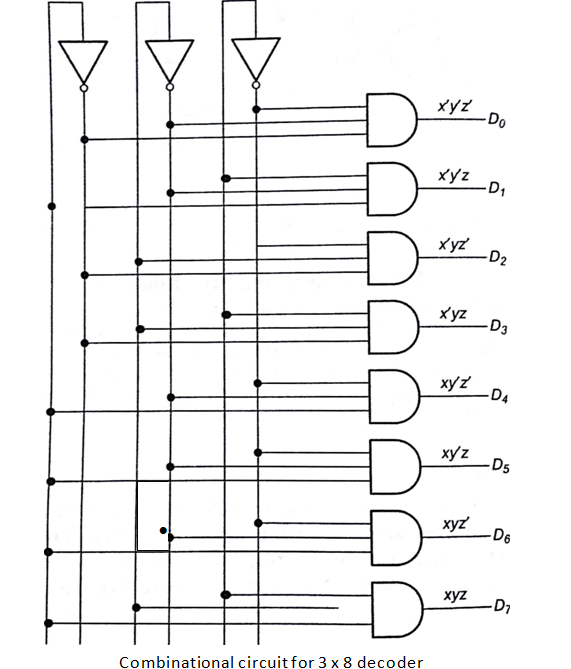
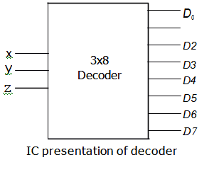
Decoders
A decoder is a combinational circuit that converts binary information from n input lines of a maximum of 2″ unique output lines. If the n bit decoded information has unused or don’t care combinations, the decoded output will have less than 2″ outputs. The decoders are also called as n to m line
decoders where m < 2″.
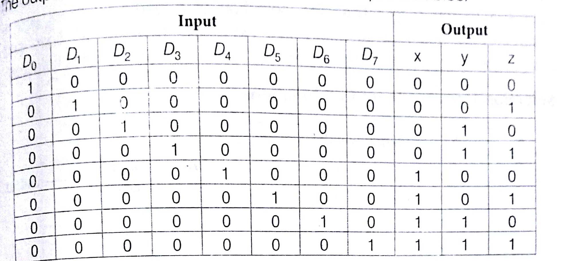
Truth Table of 3 Bit Binary to Decimal Decoder

This decoder takes binary values as input and produces decimal value output. Suppose, if D3 is high it means the binary combination of 3 that; 011, means x = 0, y = land z = 1.
x x’ y y’ z z’
 Encoder
An encoder is a digital function that produces a reverse operations from to a decoder. An encoder has 2 (or less) input lines and n output lines. The output lines generate the binary code for 2″ input variables,
From the above truth table, we get
x = D4 + D5 + D6 + D 7
y = D2 + D3 4– D6 + D 7
Z = 01 + 03 + D5 + D

Sorting in Design and Analysis of Algorithm Study Notes with Example
Follow Us On Cyber Point Solution Youtube Channel : Click Here
Follow Us on Social Platforms to get Updated : twiter, facebook, Google Plus
Learn More Ethical Hacking and Cyber Security click on this link. cyber security